-
Phone
86-755-21638081
-
Address
Room 508, Yonghui Building. Gushu 2 Road, Shenzhen, Guangdong, China
-
E-mail
LatestProducts

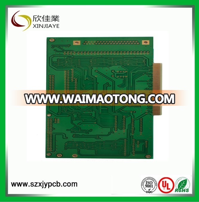
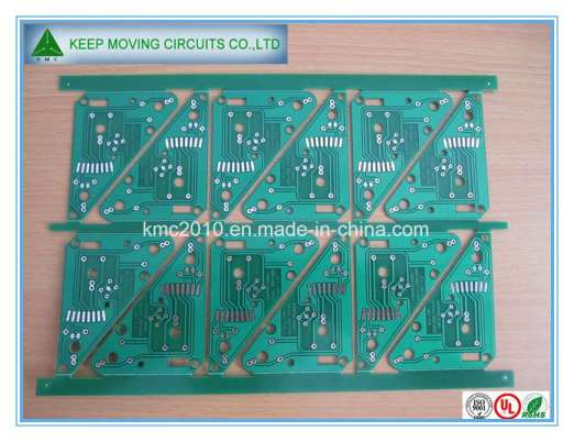
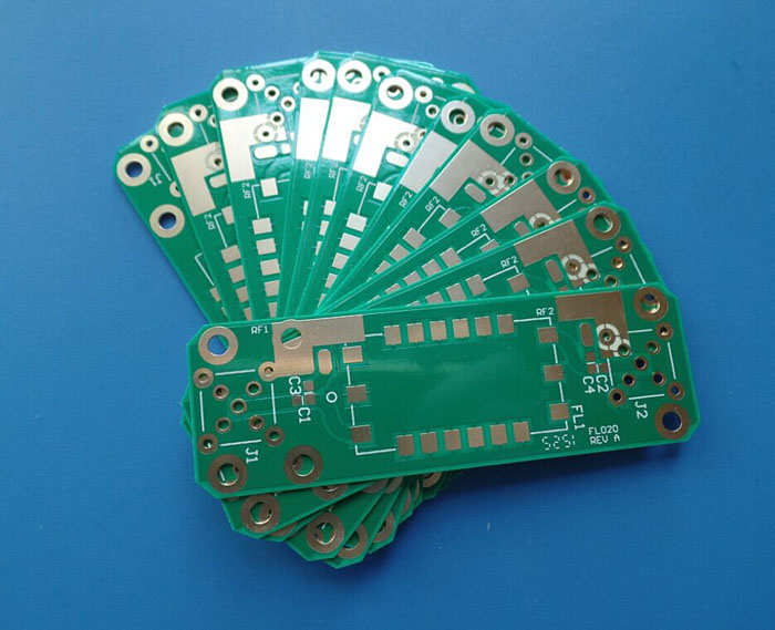
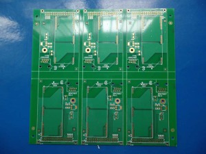
PCB for TV with UL Standard
China PCB for TV with UL Standard, Find details about China Printed Circuit Board, PCB Circuit from PCB for TV with UL Standard - Shenzhen Xinjiaye Electronics Technology Co., Ltd.
Description
Basic Info
- Model NO.: XJY-PCB 040
- Dielectric: FR-4
- Application: TV
- Processing Technology: Electrolytic Foil
- Base Material: Fr4
- Surface Finishing: Nickel/Gold Plating/Silver Entek/Hot Air
- Board Thickness: 1.2mm
- Min. Line Width: 0.075mm
- Layer: 2
- Legend Mask: White
- Trademark: XJY
- Origin: China
- Structure: Double-Sided Rigid PCB
- Material: Polyester Glass Fiber Mat Laminate
- Flame Retardant Properties: V0
- Production Process: Semi-Additive Process
- Insulation Materials: Epoxy Resin
- Copper Thickness: 1oz
- Min. Hole Size: 0.25mm
- Min. Line Spacing: 0.25mm
- Solder Mask: Green
- Package: Vacuum
- Specification: Normal
- HS Code: 85340090
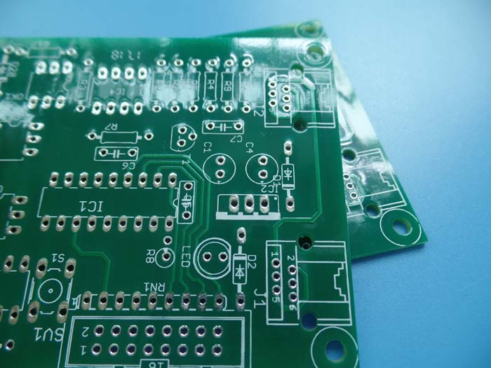
Product Description
PCB for TV with UL Standard
Our PCB board manufacture
* PCB board file with parts list provided by customers
* PCB board made, circuit board parts purchased by us
* Electronic testing circuit board
* Fast delivery, anti-static package
* RoHS Directive-compliant, lead-fre
Testing Procedures For PCB Board
---We perform multiple quality assuring procedures before shipping out any PCB board. These include:
* Visual Inspection
* Flying probe
* Bed of nails
· * Impedance control
· * Solder-ability detection
* Digital metallograghic microscope
· *AOI (Automated Optical Inspection)
Detailed Terms for PCB Manufacturing
---Technical requirement for PCB assembly:
* Professional Surface-mounting and Through-hole soldering Technology
* Various sizes like 1206, 0805, 0603 components SMT technology
* ICT(In Circuit Test), FCT(Functional Circuit Test) technology.
* PCB Assembly With UL, CE, FCC, RoHS Approval
* Nitrogen gas reflow soldering technology for SMT.
* High Standard SMT&Solder Assembly Line
* High density interconnected board placement technology capacity.
////////////////////////////////////////////////////////////////////////////////////////////////////////////////////////////
Delivery Time for PCB board
1) PCB production time: Sample: 3-4 days / mass production: Within 7 days
2) Component purchase: 2 days if all components is available in our domestic market.
3) PCB Assembly: Samples: Whthin 2 days / mass production: Within 5 days
//////////////////////////////////////////////////////////////////////////////////////////
Quotation Requirement and Time:
1) Following specifications are needed for quotation:
A) Base material:
B) Board thickness:
C) Copper thickness:
D) Surface treatment:
E) color of solder mask and silkscreen:
F) Quantity
2) Qutoation within 2 hour after we get the gerber file or PCB file with complete specifications
Shipping Method and Payment terms:
1. By DHL, UPS, FedEx, TNT using clients account.
2. We suggest you using our DHL, UPS, FedEx, TNT forwarder.
3. By EMS (Usually for Russia Clients), price is high.
4. By sea for mass quantity according to customer's requirement.
5. By customer's Forwarder
6. By Paypal, T/T, West Union, etc.
If you have any inquiry,welcome to contact Betsy!The e-mail address is :sales-betsy@xjypcb.cn
Welcome to our website !! SZXJYPCB
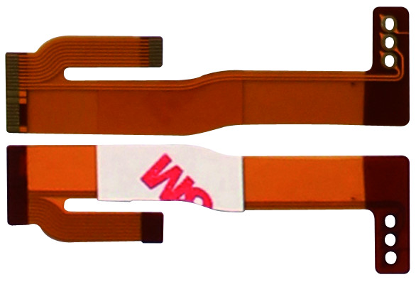
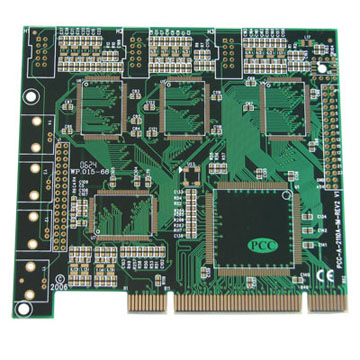
XinJiaye is able to offer one stop 1 to 24 Layer PCB fabrication,PCB manufacturing,component sourcing,
PCB Assembly,PCBA Test,Reverse engineering service;FPC fabrication, Aluminium base fabrication,
High Frequency Board fabrica-tion.
Quick Details
| Place of Origin: | Brand Name: | Model Number: | |||
| Base Material: | Copper Thickness: | Board Thickness: | |||
| Min. Hole Size: | Min. Line Width: | Surface Finishing: | |||
| PCB: |
Our PCB board manufacture
* PCB board file with parts list provided by customers
* PCB board made, circuit board parts purchased by us
* Electronic testing circuit board
* Fast delivery, anti-static package
* RoHS Directive-compliant, lead-fre
Testing Procedures For PCB Board
---We perform multiple quality assuring procedures before shipping out any PCB board. These include:
* Visual Inspection
* Flying probe
* Bed of nails
· * Impedance control
· * Solder-ability detection
* Digital metallograghic microscope
· *AOI (Automated Optical Inspection)
Detailed Terms for PCB Manufacturing
---Technical requirement for PCB assembly:
* Professional Surface-mounting and Through-hole soldering Technology
* Various sizes like 1206, 0805, 0603 components SMT technology
* ICT(In Circuit Test), FCT(Functional Circuit Test) technology.
* PCB Assembly With UL, CE, FCC, RoHS Approval
* Nitrogen gas reflow soldering technology for SMT.
* High Standard SMT&Solder Assembly Line
* High density interconnected board placement technology capacity.
////////////////////////////////////////////////////////////////////////////////////////////////////////////////////////////
Technology capability
| Items | Single/Double-sided Board/Multilayer Board/FPC(1-24Layer) | ||
| Base Materials | FR-4(High TG 150°-170°),FR1,Aluminum,CEM-3,BT,94vo | ||
| Finish copper thickness | Outer 6 OZ,Inner 4 OZ | ||
| Surface finish | ENIG, ImAg, ImSn, OSP, HASL,Plating gold | ||
| Finished Board Size | Max Double-sided Board | 640mm χ 1100mm | |
| Max Multilayer Board | 640mm χ 1100mm | ||
| Finished Board Hole Size (PTH Hole) | Min Finished Board Hole Size | 0.15mm | |
| Conductor Width and Spacing | Min Conductor Width | 0.01mm | |
| Min Conductor Spacing | 0.01mm | ||
| Thickness of Plating and Coating Layer | PTH Wall Copper Thickness | >0.02mm | |
| Tin Solder Thickness ( Hot Air Leveling ) | >0.02mm | ||
| Nickl/Gold Thickness | For customer special need | ||
| Nickl Plating Layer | >2um | ||
| Gold Plating Layer | >0.3um | ||
| Bare Board Test | Single Side Test | Max Test Point | 20480 |
| Max Board Test Size | 400mm χ 300mm | ||
| Double Side Test | Max Test Point | 40960(General Use) | |
| 4096(Special Use) | |||
| Max Board Test Size | 406mm χ 325mm | ||
| 320mm χ 400mm | |||
| Min Test pitch of SMT | 0.5mm | ||
| Test Voltage | 10-250V | ||
| Mechanical Process | Chamfer | 20°, 30°, 45°, 60° | |
| Angle Tolerance | ± 5° | ||
| Deepness Tolerance | ± 0.20mm | ||
| V-Cut Angle | 20°, 30°, 45° | ||
| Board Thickness | 0.1-3.2mm | ||
| Residues Thickness | ± 0.025mm | ||
| Cell Paraposition Precision | ± 0.025mm | ||
| Tolerance of Out-shape Process | ± 0.1mm | ||
| Board Warp | Max Value | 0.7% | |
| Optical Plotting | Max Plotting Area | 66mm χ 558.8mm | |
| Precision | ± 0.01mm | ||
| Repetitive Precision | ± 0.005mm |
||
Delivery Time for PCB board
1) PCB production time: Sample: 3-4 days / mass production: Within 7 days
2) Component purchase: 2 days if all components is available in our domestic market.
3) PCB Assembly: Samples: Whthin 2 days / mass production: Within 5 days
//////////////////////////////////////////////////////////////////////////////////////////
Quotation Requirement and Time:
1) Following specifications are needed for quotation:
A) Base material:
B) Board thickness:
C) Copper thickness:
D) Surface treatment:
E) color of solder mask and silkscreen:
F) Quantity
2) Qutoation within 2 hour after we get the gerber file or PCB file with complete specifications
Shipping Method and Payment terms:
1. By DHL, UPS, FedEx, TNT using clients account.
2. We suggest you using our DHL, UPS, FedEx, TNT forwarder.
3. By EMS (Usually for Russia Clients), price is high.
4. By sea for mass quantity according to customer's requirement.
5. By customer's Forwarder
6. By Paypal, T/T, West Union, etc.
If you have any inquiry,welcome to contact Betsy!The e-mail address is :sales-betsy@xjypcb.cn