-
Phone
86-755-21638081
-
Address
Room 508, Yonghui Building. Gushu 2 Road, Shenzhen, Guangdong, China
-
E-mail
LatestProducts

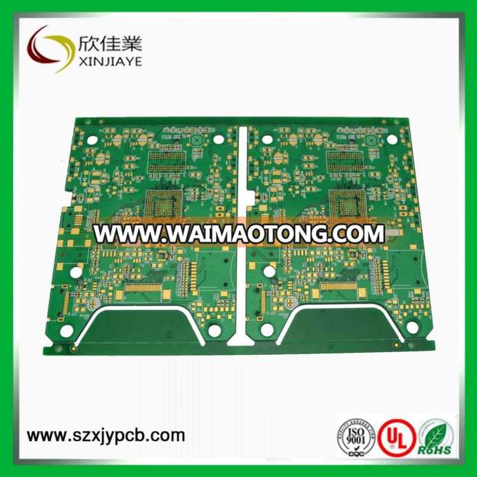
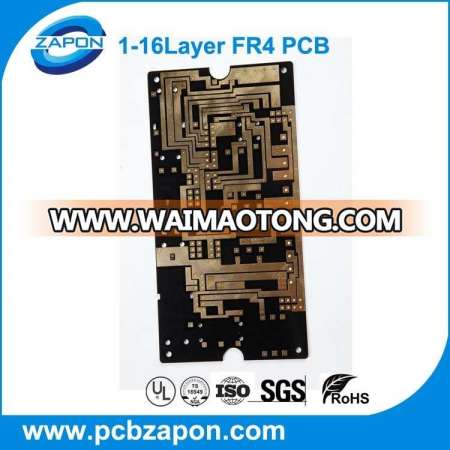
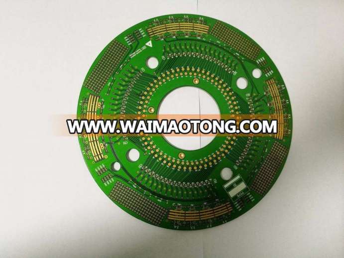
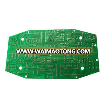
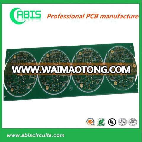
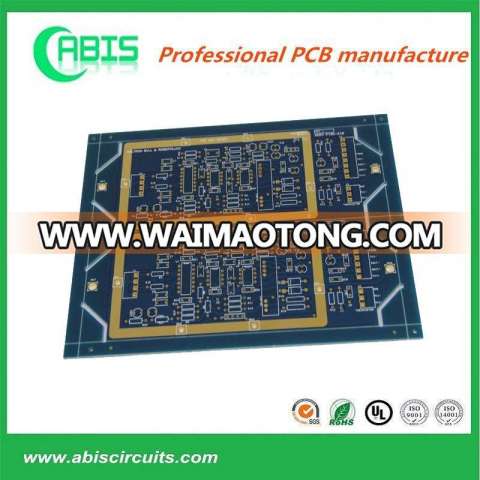
Immersion Gold PCB Manufacture in China
Immersion Gold PCB Manufacture in China, Find details about China Printed Circuit Board, Immersion Gold Pcb from Immersion Gold PCB Manufacture in China - Shenzhen Xinjiaye Electronics Technology Co., Ltd.
Description
Basic Info
- Model NO.: XJY-PCB 030
- Material: Polyimide
- Application: Digital Products, Computer with LCD Screen, Mobile Phone, Aviation and Aerospace, Electronic Products
- Flame Retardant Properties: V0
- Base Material: Fr4
- Brand: FPC
- Board Color: Green/Black/Red/Yellow Customized
- Design Improvement: Available
- Min.Hole Size: 0.15mm
- Max.Panel Size: 1200*750mm
- Shipping Express: DHL, UPS, TNT, Aramex, FedEx
- Specification: Normal
- HS Code: 854300
- Structure: Double-Sided FPC
- Combination Mode: Adhesive Flexible Plate
- Conductive Adhesive: Conductive Silver Paste
- Processing Technology: Immersion Gold
- Insulation Materials: Organic Resin
- Board Size: Customized
- Silkscreen Color: Green/Black/Red/Yellow Customized
- Min. Line Space: 0.1mm
- Min.Line Width: 0.1mm
- Certificates: ISO, UL, SGS, RoHS
- Trademark: XJY
- Origin: China
Product Description
Immersion Gold PCB manufacture in China
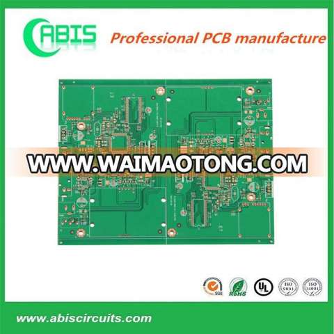
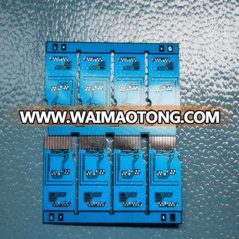
Shenzhen Xinjiaye Electronics Technology Co., Ltd is a professional pcb manufacturer has over 10 years experience. We are able to offer 1 to 24 Layer PCB, ranging from pcb produce, components purchase, pcb assembly, pcb copy service.Our products are widely used in communication apparatus, automobile electronics, auto parts, computers, medical devices, light systems, outdoor systems, network devices and consumer electronics class fields.
=================================================
Our PCB board manufacture and PCB assembly service:
1. PCB board file with parts list provided by customers
2. PCB board made, circuit board parts purchased by us
3. High Quality, competitive Price & Best Service
4.100% E-tested PCB
Testing Procedures For PCB Board:
---We perform multiple quality assuring procedures before shipping out any PCB board. These include:
* Visual Inspection
* Flying probe
* Impedance control
* Solder-ability detection
* Digital metallograghic microscope
* AOI (Automated Optical Inspection)
<<<<<<<<<<<<<<<<<<<<<<<<<<<<<<<<<<<<<<<<<<<<
Quotation Requirement:
--- Following specifications are needed for quotation:
A) Base material
B) Board thickness
C) Copper thickness
D) Surface treatment
E) color of solder mask and silkscreen
F) Quantity
Delivery Time for PCB board:
1) PCB production time: Sample: 3-4 days / mass production: Within 7 days
2) Component purchase: 2 days if all components is available in our domestic market.
3) PCB Assembly: Samples: Whthin 2 days / mass production: Within 5 days
!!!!!!!!!!!!!!!!!!!!!!!!!!!!!!!!!!!!!!!!!!!!!!!!!!!!!!!!!!!!!!!!!!!!!!!!!!!!!!!!!!!!!!!!!!!!!!!!!!!!!!!!!!!!!!!!!!!!!!!!!!!!!!!!!!!!!!!!!!!!!!!!!!!!!!!!!!!!!!!!!!!!!!!!!!!!!!!!!!!!!!!!!!!!!!!
Technology capability
Shipping Method and Payment terms:
1. By DHL, UPS, FedEx, TNT using clients account.
2. We suggest you using our DHL, UPS, FedEx, TNT forwarder.
3. By EMS (Usually for Russia Clients), price is high.
4. By sea for mass quantity according to customer's requirement.
5. By customer's Forwarder
6. By Paypal, T/T, West Union, etc.
Shenzhen Xinjiaye Electronics Technology Co., Ltd is a professional pcb manufacturer has over 10 years experience. We are able to offer 1 to 24 Layer PCB, ranging from pcb produce, components purchase, pcb assembly, pcb copy service.Our products are widely used in communication apparatus, automobile electronics, auto parts, computers, medical devices, light systems, outdoor systems, network devices and consumer electronics class fields.
=================================================
Our PCB board manufacture and PCB assembly service:
1. PCB board file with parts list provided by customers
2. PCB board made, circuit board parts purchased by us
3. High Quality, competitive Price & Best Service
4.100% E-tested PCB
Testing Procedures For PCB Board:
---We perform multiple quality assuring procedures before shipping out any PCB board. These include:
* Visual Inspection
* Flying probe
* Impedance control
* Solder-ability detection
* Digital metallograghic microscope
* AOI (Automated Optical Inspection)
<<<<<<<<<<<<<<<<<<<<<<<<<<<<<<<<<<<<<<<<<<<<
Quotation Requirement:
--- Following specifications are needed for quotation:
A) Base material
B) Board thickness
C) Copper thickness
D) Surface treatment
E) color of solder mask and silkscreen
F) Quantity
Delivery Time for PCB board:
1) PCB production time: Sample: 3-4 days / mass production: Within 7 days
2) Component purchase: 2 days if all components is available in our domestic market.
3) PCB Assembly: Samples: Whthin 2 days / mass production: Within 5 days
!!!!!!!!!!!!!!!!!!!!!!!!!!!!!!!!!!!!!!!!!!!!!!!!!!!!!!!!!!!!!!!!!!!!!!!!!!!!!!!!!!!!!!!!!!!!!!!!!!!!!!!!!!!!!!!!!!!!!!!!!!!!!!!!!!!!!!!!!!!!!!!!!!!!!!!!!!!!!!!!!!!!!!!!!!!!!!!!!!!!!!!!!!!!!!!
Technology capability
|
Items |
Single/Double-sided Board/Multilayer Board/FPC(1-24Layer) | ||
| Base Materials | FR-4(High TG 150°-170°),FR1,Aluminum,CEM-3,BT,94vo | ||
| Finish copper thickness | Outer 6 OZ,Inner 4 OZ | ||
| Surface finish | ENIG, ImAg, ImSn, OSP, HASL,Plating gold | ||
| Finished Board Size | Max Double-sided Board | 640mm χ 1100mm | |
| Max Multilayer Board | 640mm χ 1100mm | ||
| Finished Board Hole Size (PTH Hole) | Min Finished Board Hole Size | 0.15mm | |
| Conductor Width and Spacing | Min Conductor Width | 0.01mm | |
| Min Conductor Spacing | 0.01mm | ||
| Thickness of Plating and Coating Layer | PTH Wall Copper Thickness | >0.02mm | |
| Tin Solder Thickness ( Hot Air Leveling ) | >0.02mm | ||
| Nickl/Gold Thickness | For customer special need | ||
| Nickl Plating Layer | >2um | ||
| Gold Plating Layer | >0.3um | ||
| Bare Board Test | Single Side Test | Max Test Point | 20480 |
| Max Board Test Size | 400mm χ 300mm | ||
| Double Side Test | Max Test Point | 40960(General Use) | |
| 4096(Special Use) | |||
| Max Board Test Size | 406mm χ 325mm | ||
| 320mm χ 400mm | |||
| Min Test pitch of SMT | 0.5mm | ||
| Test Voltage | 10-250V | ||
| Mechanical Process | Chamfer | 20°, 30°, 45°, 60° | |
| Angle Tolerance | ± 5° | ||
| Deepness Tolerance | ± 0.20mm | ||
| V-Cut Angle | 20°, 30°, 45° | ||
| Board Thickness | 0.1-3.2mm | ||
| Residues Thickness | ± 0.025mm | ||
| Cell Paraposition Precision | ± 0.025mm | ||
| Tolerance of Out-shape Process | ± 0.1mm | ||
| Board Warp | Max Value | 0.7% | |
| Optical Plotting | Max Plotting Area | 66mm χ 558.8mm | |
| Precision | ± 0.01mm | ||
| Repetitive Precision | ± 0.005mm |
||
Shipping Method and Payment terms:
1. By DHL, UPS, FedEx, TNT using clients account.
2. We suggest you using our DHL, UPS, FedEx, TNT forwarder.
3. By EMS (Usually for Russia Clients), price is high.
4. By sea for mass quantity according to customer's requirement.
5. By customer's Forwarder
6. By Paypal, T/T, West Union, etc.
| PCB | Fastest | Nomal |
| 1layer | 1days | 4days |
| 2layer | 2days | 5days |
| 4layer | 4days | 7days |
| 6layer | 5days | 9days |
| 8layer | 6days | 10days |